
REAL-TIME FPGA-BASED IMAGE RECTIFICATION SYSTEM
Cristian Vancea, Sergiu Nedevschi, Mihai Negru
Computer Science Department, Technical University of Cluj-Napoca, Gh. Baritiu 28, 400027, Cluj-Napoca, Romania
Stefan Mathe
Computer Science Department, University of Toronto, Toronto, Canada
Keywords: Image rectification, Pipeline hardware design, VHDL, FPGA.
Abstract: Image rectification is the process of transforming stereo-images as if they were captured using a canonical
stereo-system. Computationally intensive tasks, like dense stereo matching, are greatly simplified if
performed on rectified images. We developed an efficient pipeline hardware machine which performs real-
time image rectification. The design was implemented using VHDL, thus allowing portability on many
hardware platforms. The architecture was highly optimized, both in terms of time and resources needed. To
increase its flexibility, the design was described based on generics (configuration parameters), which allow
reconfiguring different characteristics and behaviour, such as: image size, number of precision bits, memory
cache complexity. We also analyze the performance of the implemented solution on a VirtexE600 FPGA
device.
1 INTRODUCTION
The process of generating dense disparity maps
using stereo-images is a computationally intensive
task. It involves finding for every pixel in one
image, the correspondent pixel in the other image(s).
Correct corresponding point is defined as the pixel
representing the same physical point in the scene.
Normally this is a 2-D search problem, but it can be
reduced to a 1-D search problem if the images were
captured using a canonical stereo-system, almost
impossible to obtain in practice. However it is
possible to apply a rectification process over the
images, which will make them appear as if they
were captured using a canonical configuration. The
rectified images can be thought of as captured by a
new stereo-system, obtained by rotating the original
cameras around their optical centers.
Image rectification consists in transforming the
images so that the epipolar lines are aligned
horizontally or vertically.
The rectification process can be divided in two
major steps:
1. offline calculation of rectification matrices
for each camera – performed once for a
given calibrated stereo-system;
2. online image rectification from sequence to
sequence.
As the second phase is time consuming, a need to
be performed by additional hardware is encountered.
In this purpose, current paper introduces a pipeline
oriented hardware architecture, which was
implemented in a FPGA module and performs
online image rectification. The hardware
architecture is described using VHDL, the image
resolution can be dynamically set using generics
(configuration parameters) and the entire module is
technology independent though it can be ported on
any FPGA device. In this context we are able to take
advantage of the great speed technology that appears
on market, processing time being strictly dependent
on it.
2 RELATED WORK
Most of the previously stereovision hardware
machines that appeared in literature had as purpose
other tasks which involved image rectification as a
pre-processing step. Moreover they don’t really
mention any details about the rectification method
used within this step, nor specific description about
93
Vancea C., Nedevschi S., Negru M. and Mathe S. (2006).
REAL-TIME FPGA-BASED IMAGE RECTIFICATION SYSTEM.
In Proceedings of the First International Conference on Computer Vision Theory and Applications, pages 93-100
DOI: 10.5220/0001369500930100
Copyright
c
SciTePress

the hardware design. However, Fusiello, Trucco and
Verri (1997) and Fusiello (1998b) present a
rectification process based on constraints imposed
on the rectified images: principal point in position
(0,0), equal focal lengths, unchanged optical centers.
A similar method was presented later (Fusiello,
Trucco and Verri, 1998a), (Fusiello, Trucco and
Verri, 2000). It has the same principles as the
previous one, but the constraints differ a little.
A general purpose reconfigurable computer, the
PARTS system (
Woodfill and Herzen, 1997), consists
of 16 tightly coupled Xilinx 4025 FPGAs and 16
1MB SRAMs. Used for the task of stereovision, the
system achieves a performance of 42 fps at
computing 24 disparities on 320x240 pixel images.
The team from Tyzx developed a hardware
system for stereo depth computation implemented in
ASIC (Woodfill, Gordon and Buck, 2004). The
design is based on a highly parallel pipelined
architecture. It uses a pair of two stereo cameras
which connect directly to the board, though the
latency is reduced and the PCI Bus and memory are
not burdened with image data. Each camera is
calibrated to define basic imager and lens
parameters, which are used to rectify the images.
Jia et al (2004) introduce a miniature
stereovision system which generates high-resolution
disparity maps using a trinocular system attached to
a hardware module implemented in FPGA. Its
frequency is 60 MHz, reaching up to 30 fps. The
depth is calculated using 64 disparity levels and 256
disparity levels with interpolation. Epipolar
rectification is used in order to simplify the stereo
correspondence.
3 IMAGE RECTIFICATION
METHODOLOGY
The idea behind image rectification consists in
calculating a rectification matrix, for each camera,
based on the Perspective Projection Matrices
characterizing both original (P
o
) and defined
canonical (P
c
) stereo systems. Knowing the point
coordinates in the original image (
o
i
) and the optical
centre (c) of the camera, its correspondent point in
World Reference Frame (WRF) is:
oo
iQcw ⋅+=
−1
(1)
where:
T
oooo
Svu ],,[=i
T
ZYX ],,[=w
[]
ooo
qQP |=
Considering the projection formula from WRF
onto the rectified image (obtained without moving
the optical centre of the camera), the new position of
the image point becomes:
[]
()
iQQqcQi
qiQcQ
w
qQ
w
Pi
oocccr
coocccc
r
⋅⋅++⋅=
⇒+⋅+⋅=
⎥
⎦
⎤
⎢
⎣
⎡
⋅=
⎥
⎦
⎤
⎢
⎣
⎡
⋅=
−
−
1
1
1
|
1
(2)
where:
T
rrrr
Svu ],,[=i
0
=
+
⋅
cc
qcQ
– optical centre is projected in (0,0)
In this way the corresponding position in
rectified image can be calculated for each pixel from
original image:
o
ooc
r
iTiQQi ⋅=⋅⋅=
−1
(3)
where:
1−
⋅=
oc
QQT
– rectification matrix
It has to be stated that rectifying an image is not
a simple product between the rectification matrix
and the vector representing the current pixel
coordinates in the image. Practically the image
coordinates are integer values and the elements of
the rectifying matrix are real numbers. The
approximation of the corresponding points
coordinates could distort the rectified image. So for
each integer coordinate of the rectified image the
corresponding point onto the original image is
computed using the inverse of the rectifying matrix:
u
o
= t
11*
u
r
+ t
12*
v
r
+ t
13
(4)
v
o
= t
21*
u
r
+ t
22*
v
r
+ t
23
(5)
where:
i
o
= (u
o
, v
o
, 1)
T
– point coordinates in original image
i
r
= (u
r
, v
r
, 1)
T
– point coordinates in rectified image
⎥
⎥
⎥
⎦
⎤
⎢
⎢
⎢
⎣
⎡
=
332331
232221
131211
ttt
ttt
ttt
1-
T
Such a point will have real coordinates and will
be situated between four pixels (fig. 1). In order to
maintain clarity, a bilinear interpolation of the four
neighbouring pixels’ intensities will give the
resulting intensity in the rectified image:
u
o
= u + d
u
(6)
v
o
= v + d
v
(7)
I
r
(u
r
,v
r
) = I
o
(u,v)*(1-d
u
)*(1-d
v
) + I
o
(u+1,v)*d
u
*(1-d
v
)
+ I
o
(u,v+1)*(1-d
u
)*d
v
+ I
o
(u+1,v+1)*d
u
*d
v
(8)
where:
I
r
– rectified image intensity bitmap
I
o
– original image intensity bitmap
VISAPP 2006 - IMAGE FORMATION AND PROCESSING
94
original image
(u,v+1) (u+1,v+1)
(u+1,v)(u,v)
1−
T
rectified image
),(
rr
vu
u
d
v
d
Figure 1: Image rectification methodology.
4 HARDWARE DESIGN
There are some issues to be discussed before giving
any details about the hardware architecture. First of
all the entire architecture was described using
VHDL. For that reason, some features could be
described using generics: image dimension, image
area to be rectified, precision. The inverse of
rectification matrix is also given using generics. The
design can be optimized in matters of speed and
resources to be used inside the FPGA device. Using
generics, one can choose for a complex design
handling more situations, giving greater precision in
results, or choose for a simpler design which would
need fewer resources, but would handle less
situations or even worse precision.
The input consists in the original image and the
output will be the rectified image. Practically, the
process consists in parsing the rectified image pixel
by pixel and applying the equations (4), (5) and (8)
in order to determine their intensity. The hardware
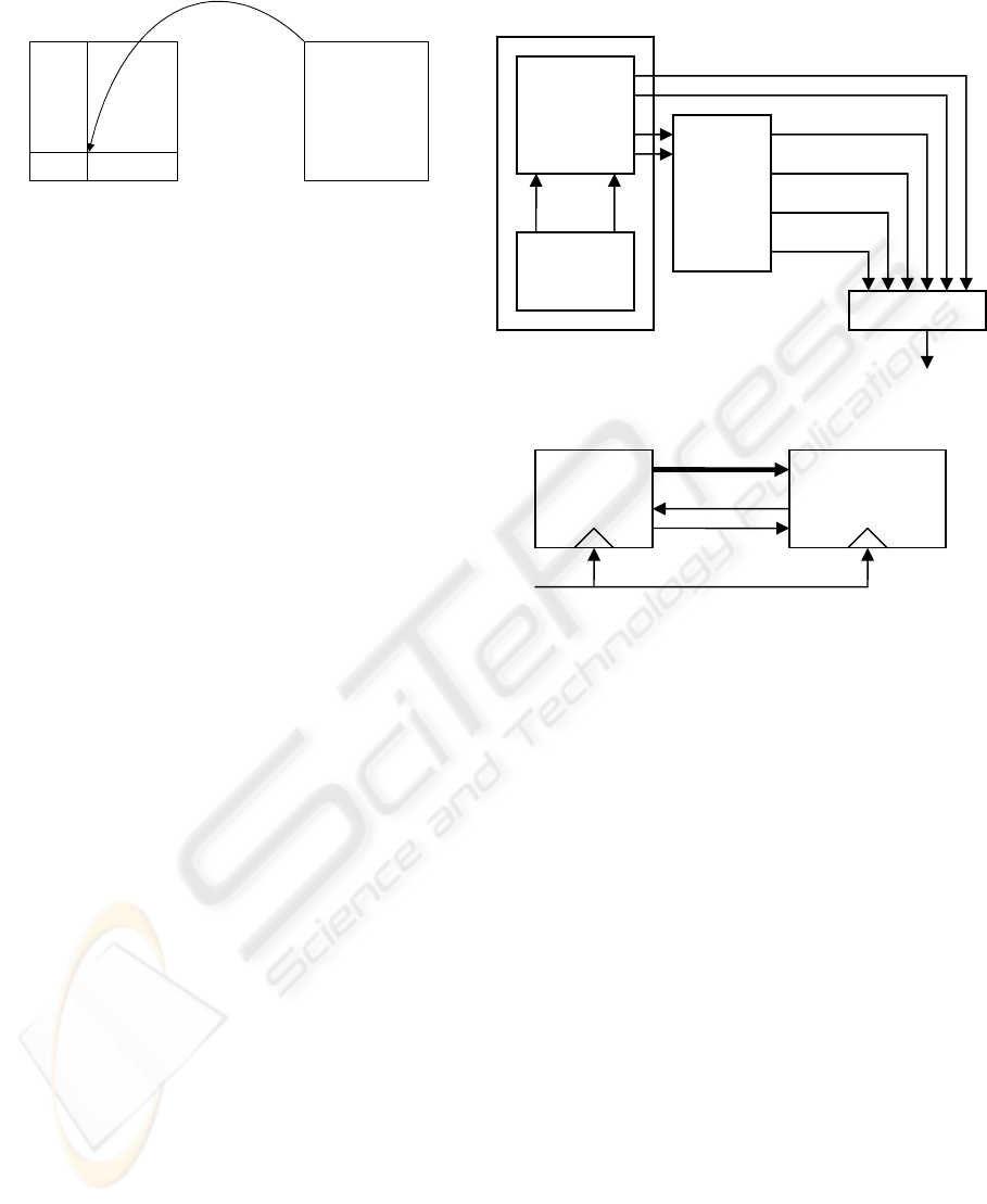
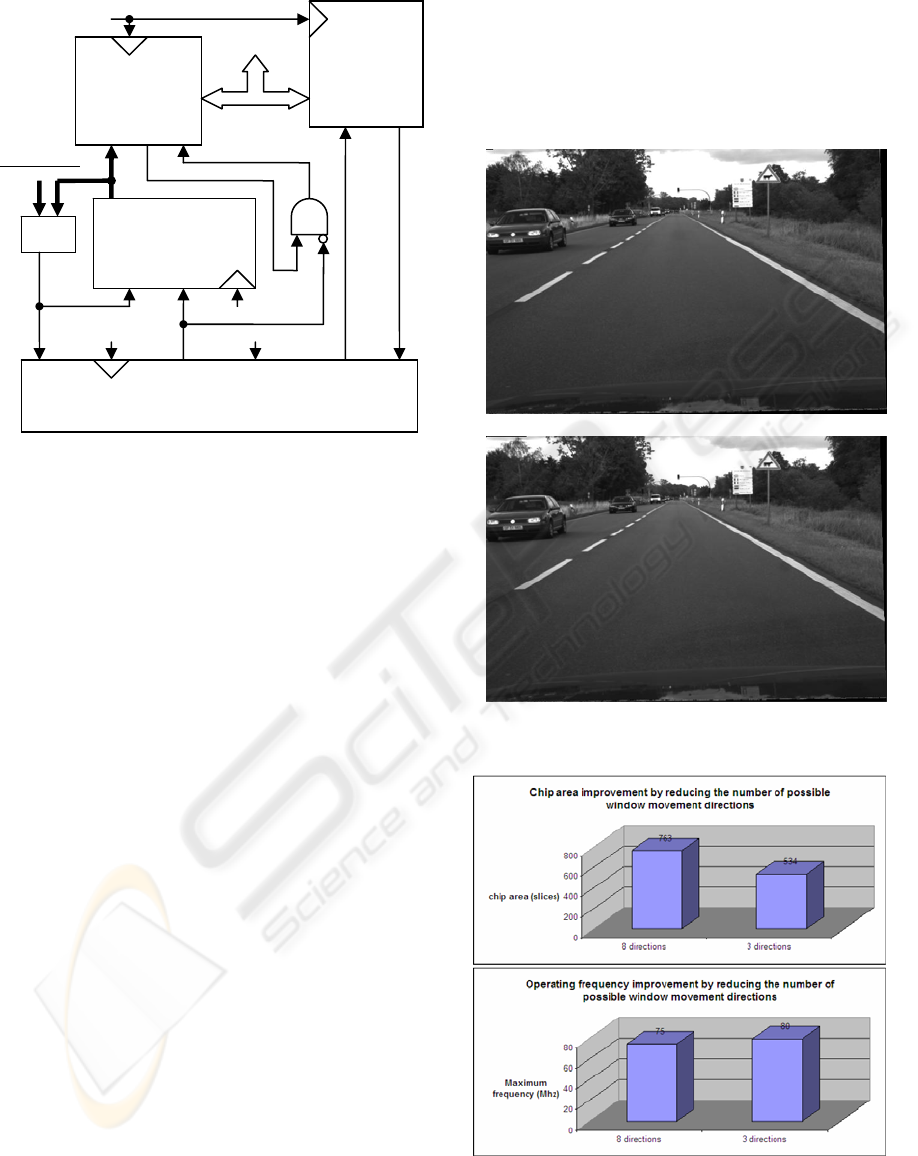
architecture was divided in three major parts (fig. 2):
• coordinate generator and 2-D
transformation block;
• source image reader;
• interpolator.
4.1 Communication Protocol
Each of the three blocks is an independent pipeline
module. They communicate using a very simple
one-way communication protocol called DFLOW
(Data FLOW – fig. 3).
The handshaking is simple: when source has
valid data, it outputs the data onto the DATA bus
and enables the WEN signal; when destination is
ready to receive data it sets the RDY signal high;
when both RDY and WEN are set, data transfers
take place on each clock cycle. In this way,
continuous transfer is possible.
Figure 2: Image rectification hardware architecture.
Figure 3: DFLOW communication protocol.
4.2 Coordinate Generator and 2-D
Transformation Block
This part of the architecture has as purpose the
calculation of u, v, d
u
and d
v
using formulas (4) and
(5). As the relations are similar, the same hardware
unit can be duplicated to perform all operations. We
will discuss further how to implement relation (4).
It can be noticed that only adders and multipliers
should be involved, but multipliers are slow and
complex modules. Another observation is that u
r
and
v
r
are increasing by 1 and rectification matrix
elements are real number constants, though it is
possible to perform multiplication by using repeated
sums, on each clock cycle and storing the temporary
result in a buffer (see fig. 4).
Any unit of the module, which is driven by a
clock signal, contains a register on the output. Such
a measurement was taken in order to insert fast
stages in the pipeline. As the entire architecture was
designed to work with integers, generics like t
11
, t
12
,
t
13
had to be shifted to the left with a certain number
of precision bits. This number varies depending on
the stage of the pipeline architecture. For example,
Source
Destination
RDY
WEN
DATA
CLK
Coord.
generator
2-D
Transform
Block
v
r
u
r
Source
Image
Reader
u
v
d
v
d
u
I
o
(u+1,v)
I
o
(u,v)
I
o
(u,v+1)
I
o
(u+1,v+1)
Inter
p
olato
r
I
r
(u
r
,v
r
)
REAL-TIME FPGA-BASED IMAGE RECTIFICATION SYSTEM
95
in the first stage where t
11
and t
12
are summed
repeatedly for a certain number of times, more
precision bits are needed than the stage where t
13
is
added. The idea is to use only k precision bits when
calculating u
r
*t
11
and v
r
*t
12
and only l (smaller than
k) precision bits when performing the rest of the
sums. In this way a lot of FPGA resources will be
saved for other purposes. It can be proved that for f
precision bits wanted in the final result, k and l
should respect the following relations, so as to
obtain the optimal solution in terms of resources
required:
l = f + 4 (9)
k = f + 2 + log
2
(W + H) (10)
where:
W, H – image weight and height
Figure 4: Coordinate generator and 2-D transformation
block.
The design in figure 4 is configured using a set
of generics:
• t
11
, t
12
, t
13
– first raw of rectification matrix;
• i – number of bits to represent the integer
part of the result;
• f – number of bits to represent the fractional
part of the result;
• image width.
The output lines are:
• Finished – is asserted when the entire
image was rectified;
• Overflow – is asserted when the resulting
position in the original image is outside;
• Result – represents the result data bus; it is
represented using i + f bits.
4.3 Source Image Reader
The large amount of storage space needed for
memorizing the acquired frames in a stereo vision
system well exceeds the capabilities of internal
BRAM units. The solution is to use external
memories, which, in most cases, are either SRAM or
SDRAM. The former has the advantage of
simplified access, while the latter has a higher
capacity. Since many of the FPGA-PCI boards
present on the market today provide SDRAM
modules for external storage, we designed a
component that can efficiently fetch the pixels to be
used as the input for the interpolator.
The input of the image reader component
consists of a stream of pairs of pixels coordinates in
the image space. For each such pair of coordinates,
the image reader should provide as output a tuple of
4 pixel intensities, corresponding to a 2x2 window
whose top-left corner is located at these coordinates
in the image that is stored inside the external
storage.
The difficulty of the task resides not in fetching
the pixel values, but rather doing this in an efficient
manner. It can be noticed that while the window
sweeps the image, it usually does so by moving in
successive partially overlapping positions. Even
more conveniently, data is stored inside the SDRAM
in 32-bit words, that is, 4 successive pixels are
accessible by performing one read operation. As a
consequence, it is possible to build an efficient cache
that can both provide pixels at a much higher rate
and can also significantly reduce the memory load.
The cache will store a window of 2x2 32-bit
words (16 pixels) from the image. The operations
performed by the cache will be:
• read a 32 bit word into one of the positions
of the cache;
• shift the cache in one of the 8 possible
directions;
• send the contents of a 2x2 pixel window
over the output port.
The phases of the computation performed inside
the image reader module are described in what
follows (fig. 5):
Image
width
FULL
Counter (u
r
)
t
11
Register
RST
+
Clk
t
11
*u
r
Sign
ext.
Sign
ext.
Cl
k
Finished
Overflow
Result (u
o
)
Register
FULL
Counter (v
r
)
t
12
Register
RST
+
Clk
t
12
*v
r
Sign
ext.
+
Cl
k
t
13
+
Cl
k
Sign
ext.
≤
Cl
k
VISAPP 2006 - IMAGE FORMATION AND PROCESSING
96
Window tracking involves detecting the direction
in which the 2x2 pixel window moves relative to its
previous position. It is a two stage pipeline process,
in which the difference between the new and old
coordinates is computed on a per-axis basis.
Differences corresponding to -1, 0 and +1 are
detected and encoded using a direction encoder,
described in table 1.
Table 1: Direction encoding.
RST U- U0 U+ V- V0 V+ DIR
1 X X X X X X NEW
0 0 1 0 0 1 0 SAME
0 0 0 1 0 1 0 0
0
0 0 0 1 1 0 0 45
0
0 0 1 0 1 0 0 90
0
0 1 0 0 1 0 0 135
0
0 1 0 0 0 1 0 180
0
0 1 0 0 0 0 1 225
0
0 0 1 0 0 0 1 270
0
0 0 0 1 0 0 1 315
0
0 Otherwise NEW
Figure 6: The internal structure of the cache.
Based on the coordinates of the window and the
movement direction provided by the window tracker
pipeline, command generation block has the task to
create the set of parallelized commands that should
be carried out by the cache in order to make
available all the pixels inside the window. The
output of the command generator will be:
• read – a vector of 4 bits, read(i) being set if
it is necessary to perform a read operation
for word number i in the cache (word
numbering inside the cache is depicted in
figure 6);
• shift – one of the 8 shift directions or
SHIFT_NONE if no shift needs to be
carried out;
• offset – the offset of the 2x2 pixel window
inside the cache. This will be needed for
carrying out the sending operation.
At most 4 read operations may result after the
command generation phase, corresponding to the 4
32-bit word positions in the cache. The addresses for
the 4 words can be immediately derived from the
coordinates of the 2x2 pixel window, by obtaining
the byte address (v x img_width + u) and rounding it
down to the nearest 32-bit word (fig. 7).
Figure 7: Read addresses computation.
Based on this observation, it is possible to
compute the addresses in parallel with the window
tracking and command generation phase, thus
reducing the overall pipeline length. As address
computation involves the use of one constant-
argument pipeline multiplier, we developed a highly
optimized component based on Booth's Algorithm.
The Address Generation branch and Window
Tracking + Command Generation branch (fig. 5)
might not have the same number of stages. For that
reason, a Pipeline Synchronizer based on DFLOW
handshaking protocol was introduced.
Some of the commands may not be executed in
parallel by the cache. This problem is solved using a
Figure 5: Flow Diagram for Image Reader module.
REAL-TIME FPGA-BASED IMAGE RECTIFICATION SYSTEM
97
Command Serialization unit. The following
constraints must be met:
• only one read may be performed per clock
cycle;
• cache shifting must take place before or in
the same clock cycle as the first read
operation;
• send operation must be performed after the
last read for current window position is
completed and before or in the same clock
cycle as the first read or shift for the next
window position takes place.
Due to the fact not all commands will involve a
read operation from memory, using a Command
FIFO unit will allow them to be executed while
SDRAM Controller performs readings for other
commands. The result is a speedup in the process.
The final stage of the image reader pipeline is the
cache. Its function is to process the serialized
commands coming from the Command Serialization
unit through the Command FIFO together with the
data values coming from the SDRAM Controller.
The control logic will always schedule the shift
operation in the first clock cycle after a command is
loaded (if there is no pending send command), since
it is always possible to execute it. Read operations
are scheduled as soon as the data from SDRAM
Controller becomes available. Send operations are
scheduled last, after the last read operation has been
completed. Send operations will actually be
executed some time after the last read operation,
when the output becomes ready. However, in order
to ensure continuous operation of the cache, a send
command may be pending while another command
is being loaded into the input buffers, allowing the
sending of data to be overlapped with the arrival of
the next command. Nevertheless, if the sending
operation continues to remain pending because the
destination is not ready to receive data, the next
command will not start execution. The cached data
is kept in registers which are capable of executing
the shift and read operations. The input of each of
the four 32-bit registers is connected, through a
multiplexer, to each of the other 3 registers and to
the data buffer. This is, the most expensive part of
the image reader component both in terms of
resources and propagation delay. Further
optimizations can be carried out by noticing that, in
applications like image rectification, the cache will
not be performing shift operations in all of the 8
directions, though some of the logic may be
eliminated. Boolean generics, for each window
movement direction, were introduced in the VHDL
description, to allow flexible design configuration.
4.4 Bilinear Interpolator
This is the final stage of the image rectification
architecture. It performs the bilinear interpolation of
the four neighboring intensities from the original
image, according to d
u
, d
v
offsets.
This part includes a set o adders and
multiplication modules. We modified formula (8) in
such a way that that the number of multiplication
units decrease to minimum possible. The reason is
that a multiplication module requires a lot of
pipeline stages. The more consecutive multipliers we
have, the greater the number of pipeline stages we
get. An optimized solution is presented in what
follows.
Consider the following bilinear interpolation
formula:
P = a
*(1-d
u
)*(1-d
v
) + b*d
u
*(1-d
v
) + c*(1-d
u
)*d
v
+
d*d
u
*d
v
(11)
This could be written as:
P
1
= a*(1-d
u
) + b*d
u
= a + (b-a)*d
u
(12)
P
2
= c*(1-d
u
) + d*d
u
= c + (d-c)*d
u
(13)
P = P
1
*(1-d
v
) + P
2
*d
v
= P
1
+ (P
2
-P
1
)*d
v
(14)
As formulas (12) and (13) can be performed in
parallel, the interpolation process was optimized to
only two consecutive multiplication stages. Also, the
number of needed resources was reduced because
the number of multiplication units decreased from 8
to 3.
4.5 Top-level of the Architecture
The entire rectification process was designed to have
two major phases:
1. image load into memory;
2. image transformation.
First phase consists in loading the image from
the software module into the SDRAM through the
PCI bus. For that reason, a counter generating the
address for the SDRAM is used. Communication
with memory is performed using the DFLOW
protocol. Second phase is designated for rectifying
the image in memory. The Address Generator
module is disabled and the Image Transformation
module is put at work. A description of the top-level
control unit and dataflow is presented in figure 8.
(a)
Rst
Finished=’1’ Pipe_Empty=’1’
Rst_Mem=’1’
Rst_Rectif=’0’
Rst_Mem=’0’
Rst Rectif=’1’
Rectify Image
Load Image
VISAPP 2006 - IMAGE FORMATION AND PROCESSING
98
(b)
Figure 8: Top-level view of Image Rectification System:
a) control unit; b) dataflow.
5 EXPERIMENTAL RESULTS
The hardware design was tested using a Strathnuey
board equipped with a Ballyderl DIME module
containing a Virtex FPGA (model V600EFG680)
and 128MB SDRAM. The images (640x512 pixels)
were sent from PC through the PCI bus and the
rectified images were read back into the PC,
registering a total time of 17.5 ms (57 fps). Such
amount of time is due to the fact the PCI
communication between PC and FPGA-PCI board is
very slow. Practically, the design working at a
frequency of 80 MHz, waits until the image
download and upload through PCI is performed. On
the other hand, the time required only for rectifying
the image (no upload and download) is about 4.5 ms
(222 fps). Download time can be eliminated if
images will be captured directly from camera and
not through PCI.
The resulting images were tested against those
obtained with a software reference implementation.
The similitude between both solutions can be seen in
figure 9 (dark patterns on the margins represent
pixels from the rectified image with correspondents
outside the original image).
We performed several tests concerning chip area
usage statistics. For example, by reducing the
number of possible window movement directions,
the amount of chip area and operating frequency can
be improved. In the case of the image rectification
task, the image is swept using successive lines. This
implies that the window movement direction can
take at most 3 values of the 8 possible ones. The
improvement in performance is shown in figure 10.
Chip area improvement is the most significant, from
around 11% down to around 7%.
(a)
(b)
Figure 9: Rectified images: a) hardware results; b)
software results.
Figure 10: Performance can be improved by removing
unused window movement directions.
To test the performance of the Image Reader
design, different image rotation matrices have been
Rst
Top-level FSM
Memory
(image)
Image
Rectification
Module
Rst Empty
Address generator
(counter)
Rst
Communication
BUS
Address
=
Width*Height
4
Finished Rst_Mem
Rst
Rectif
Clk
Clk
Clk
Rst
S
y
nch
RDY WEN
PCI
Pipe
Empty
Rst
REAL-TIME FPGA-BASED IMAGE RECTIFICATION SYSTEM
99
used. Figure 11 shows the variation of the
throughput (megapixels/second) as a function of the
rotation angle, measured at a 75 MHz frequency
(memory controller operating at the same
frequency).
Figure 11: The throughput of the image reader as a
function of image rotation angle at a frequency of 75
MHz.
The variation of the throughput is 14% of the
maximum value, with a minimum of 43 Mb/s
(obtained at 150
0
and 210
0
) and a maximum of 50.6
Mb/s (for 90
0
and 270
0
). It can also be noticed that
the performance for a 0
0
angle is less than the one
obtained at 90
0
. The reason is that, in the first case,
when a cache miss is found, two read operations
(corresponding to words 1 and 3 of the cache) are
requested at once by the Command Generator and
the cache must stall for one clock cycle, to perform
the second read. In the second case, a miss will
usually generate one read operation (words 2 and 3),
and will not stall the pipeline (with the exception
being the situation in which the window is in the
middle of the cache - offset 3 - in which both words
2 and 3 will require reading).
6 CONCLUSIONS AND FUTURE
WORK
A flexible and scalable solution has been developed
for the problem of image rectification, providing
real-time results with configurable parameters such
as: image resolution, number of precision bits to be
used in calculus. The possible window movement
directions can be freely configured as to reduce chip
area usage and increase accepted clock frequency.
Image quality results proved to be very close to
the ones obtained using a reference software
implementation. The description was made
independent of the underlying technology, though it
can be ported easily on other platforms.
The processing time is very small, but the
transfer of images through the PCI bus proved to be
the weakest part (tests were performed with a slow
FPGA from VirtexE family). A solution to eliminate
such inconvenience would be to link the camera
directly to the FPGA board and implement, inside
the chip, an architecture which knows the
communication protocol with the camera. In this
way, only resulting images will have to be
transferred through the PCI, thus saving a lot of
time.
An alternative solution to be investigated in the
future consists in replacing the Coordinate Generator
and 2-D Transformation blocks with a lookup table
containing (with sub-pixel precision) the position in
original image, of each pixel from rectified image.
In this case the memory workload will increase
inefficiently, though several SDRAM/SRAM
modules would be needed to avoid such
inconvenience. On the other hand, a lookup table
based system might be used for more complex
processes, like image rectification combined with
image un-distortion or ground plane stereo-
correction, which require extremely complex
operations, difficult to be implemented in a fast
pipeline fashion.
REFERENCES
Fusiello, A., Trucco, E. & Verri, A. (1997). Rectification
with unconstrained stereo geometry. In Proceedings of
the British Machine Vision Conference. University of
Essex, BMVA Press. pp. 400-409.
Woodfill, J., Herzen B. (1997). Real-time stereo vision on
the parts reconfigurable computer. In IEEE Workshop
on FPGAs for Custom Computing Machines, pp. 242-
252.
Fusiello, A., Trucco, E. & Verri, A. (1998a). Rectification
with unconstrained stereo geometry. Research
Memorandum RM/98/12. Edinburgh, Department of
Computing and Electrical Engineering, Heriot-Watt
University.
Fusiello, A. (1998b). Tutorial on rectification of stereo
images. In R. Fisher, editor, CVonline: On-Line
Compendium of Computer Vision [Online]. Available:
http://www.dai.ed.ac.uk/CVonline/
Fusiello, A., Trucco, E. & Verri, A. (2000). A compact
algorithm for rectification of stereo pairs. Machine
Vision and Applications, 12(1):16-22.
Woodfill, J.I., Gordon, G., Buck R. (2004). Tyzx DeepSea
High Speed Stereo Vision System. In Proceedings of
the IEEE Computer Society Workshop on Real Time 3-
D Sensors and Their Use, Conference on Computer
Vision and Pattern Recognition. Washington D.C.
Jia, Y., Zhang, X., Li, M. & An, L. (2004). A Miniature
Stereo Vision Machine (MSVM-III) for Dense
Disparity Mapping. In Proceedings of the 17
th
International Conference on Pattern Recognition.
Cambridge. Volume 1, pp. 728-731.
VISAPP 2006 - IMAGE FORMATION AND PROCESSING
100
